This facility has not published any Products. Please check back.
The following Products and Services are available within our facility:
Atomic Force Microscopy
 |
MFP3D
Asylum MFP-3D Standard System with Low Force Indenter
Operation Modes:
Contact and tapping (AC) mode; lateral force mode (LFM); phase imaging; electric force microscopy (EFM); nanolithography; force curve mode; ramp mode; force mapping mode.
Features:
90 micron travel in (x,y) and 15 micron in z; X-Y closed loop (non-linearity <0.5%) with sensitivity < 150pm noise; Z-closed loop (<0.2%) with sensitivity < 35pm noise; ARgyle-3D imaging in real time; AFM control program integrated with IGOR pro.
|
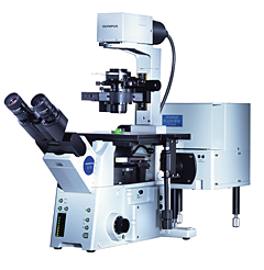 |
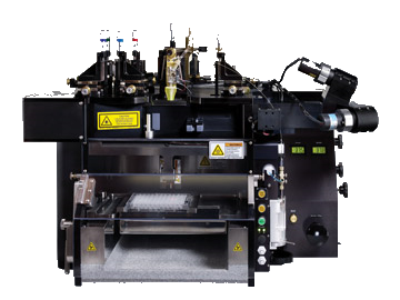
MFP3D-Bio
Asylum MFP-3D Bio
Application:
The AFM is mounted on an inverted optical microscope (Olympus IX71) and is equipped with a closed fluid cell for liquid AFM studies. It allows combined optical and atomic force microscopy on biological samples but can be used also for any other materials applications.
Operation Modes:
Contact and tapping (AC) mode; lateral force mode (LFM); phase imaging; electric force microscopy (EFM); nanolithography; force curve mode; ramp mode; force mapping mode.
|
Chemical Analysis
|
|
Cameca APT
Cameca 3000X HR Local Electrode Atom Probe (LEAP)
The Cameca LEAP Atom Probe can be operated in voltage-pulse mode, for metals and low-band-gap semiconductors, or in laser-pulse mode ( 13 ps pulse, 532 nm green laser) for wide-band-gap materials. The instrument is equipped with a reflectron providing higher energy resolution and therefore improved peak separation in the mass spectrum as compared to straight flight-path instruments; the detection efficiency is approximately 37%. Pulse rates can be adjusted up to 500 kHz. Samples are run cryogenically, as low as 25 K, to minimize the migration of surface species.
|
 |
Cameca SIMS
Cameca IMS 7f Auto SIMS
The Cameca IMS 7f Auto SIMS, purchased new in 2014, combines the extreme sensitivity and mass resolution of earlier Cameca magnetic SIMS instruments with new features making operation easier and more consistent.
The IMS 7f Auto has two primary ion sources, cesium and oxygen. Depending on the sample, it can achieve a depth resolution as low as 2 nm. Masses from 1 amu to 360 amu can be detected, and the mass resolution is sufficient toeliminate nearly all interferences. The detection limit for B in Si is 3E13/cm3.
|
 |
Kratos XPS
Kratos Axis Ultra DLD XPS
The Kratos Axis Ultra DLD XPS system is equipped with a non-monochromated Mg X-ray anode, and a monochromated Al anode. It has a charge neutralization system enabling us to achieve reliable peak positions on virtually any sample. Most elements can be detected down to 0.01 to 0.1 % atomic (100 to 1000 ppm).
The automated stage allows the machine to run unattended, taking spectra from multiple samples; individual samples up to 12 mm thick and 50 mm wide can be accommodated. The stage can be tilted up to 75 degrees to vary the depth of the measurement.
|
Focused Ion Beam Microscopy
 |
FEI Helios
FEI Helios Dualbeam Nanolab 650
The instrument is equipped with an Elstar field emission SEM for nanometer resolution imaging and a Tomahawk FIB column operating from 30kV down to 500V. Ion currents range from 7pA, providing a minimal beam size of 7nm, to 22nA which can be used for substantial milling tasks. The very stable piezo-driven stage can operate on an area of 150 x 150 mm.
Attached are currently a gas source for platinum deposition as well an Omniprobe manipulator that is typically used for transfer of TEM and APT samples.
|
|
|
Tribeam
Tri-BEAM (FEI Dualbeam Versa with Laser)
The microscopy facility houses techniques that provide 3D structural and chemical information on various lenght scales. Very roughly categorized they provide data for volumes of 100 nm (APT), 1 micron (electron tomography, TEM) and 10 micron (FIB) edge length. The Tri-beam system aims at increasing that length towards 100 micron and more.
The new instrument, developed in the research group of Prof. Tresa Pollock in the Materials Department, augments a standard FIB with a scanning femtosecond laser.
|
Scanning Electron Microscopy
 |
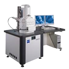
XL30
FEI XL30 Sirion FEG SEM with EBSD and EDX
High resolution scanning electron microscope completely controlled under WindowNT; equipped with a high stability Schottky field emission gun and a large specimen chamber (379x280 mm door size); Voltage: 500-30keV; Resolution: 1.2 nm @30keV.
Detectors:
Standard SE; dedicated back scattering detector for Z-imaging; Edax Si-drift EDX detector for highly efficient recording of elemental maps; Edax EBSD detector for crystallogrpahic analysis.
|
|
|
XL40
FEI XL40 Sirion FEG SEM with EDX
High resolution scanning electron microscope completely controlled under WindowNT; equipped with a high stability Schottky field emission gun and a large specimen chamber (379x280 mm door size); Voltage: 500-30keV; Resolution: 1.2 nm @30keV.
Detectors
Oxford Inca x-ray EDX system; back scattering detector for Z-imaging.
|
|
|
Inspect CL
FEI Inspect SEM with CL
Scanning electron microscope completely controlled under WindowNT; currently equipped with tungsten tip for high beam currents; large specimen chamber (379x280 mm door size). Voltage: 200 - 30 kV; Resolution: 3.0 nm @30kV; 10 nm @3kV.
Detectors:
Oxford CL2 cathodoluminescence system with cooling stage. Back scattering detector for Z-imaging.
|
Transmission Electron Microscopy
|
|
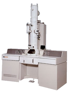
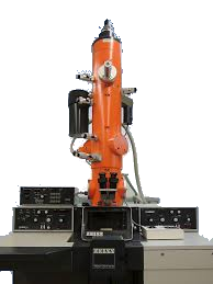
FEI T20C
FEI Tecnai G2 Sphera 200kV Cryo
(for Life Science Studies)
This microscope is equipped with a Twin objecitve lens which provides at a beam energy of 200keV a moderate resolution of 3A. It is characterized by a large pole piece gap which leaves enough space for larger sample holders such as a cryo holder. It also allows a larger tilt range and is therefore particularly suitable for nanoscale defect analysis in crystalline samples.
Features:
LaB6 emitter; CompuStage with Smart-Tilt software; Low-dose exposure modes; CCD camera (Gatan Ultrascan 1000 2k x 2k).
|
|
|
FEI T20E
FEI Tecnai G2 Sphera 200kV EDX
(for Materials Science Studies)
This microscope is equipped with a Super-Twin objective lens which provides at 200keV and the given LaB6 emitter a point resolution of 2.2A. This is suitable for basic atomic resolution TEM analysis of for example nano particles. An Oxford electron dispersive X-ray spectrosometer (EDX) allows point-to-point chemical analysis with a chemical sensitivity down to 0.2%
Holders:
(1) FEI single tilt, tilt range a=±45° (2) FEI double tilt, a=±40°, ß=±18°
|
|
|
FEI Titan 80-300
FEI Titan 80-300kV FEG TEM-STEM with EDS/EELS
(for Analytical Studies)
The Titan is the most versatile microscope which is currently the only one that can be operated both in STEM and TEM mode. Working in an energy range between 80 and 300keV and equipped with a field emission gun it can reach a spatial resolution of 1.3A in STEM, and an information limit of 0.9A in high resolution TEM mode. An energy dispersive X-ray (EDX) detector and an electron energy loss spectrometer (EELS) allow analytical work on the nanometer scale.
Features:
(1) A scanning unit with a high-angle annular dark-field (HAADF) detector for STEM (Z-contrast
|
Sample Preparation
.png) |
Vitrobot
FEI Vitrobot Mark IV
Fully automated, reproducible vitrification of suspensions; high vitrification quality through controlled environment; high sample throughput; flexible instrument control; semi-automated grid transfer.
|
 |
Pips
Gatan Precision Ion Polishing System (Model 691)
|
 |
Fischione
Fischione Ion Mill (Model 1010)
|
This facility has not published any News. Please check back.
Quick Quotes have not been configured. Please check back soon (Code 001, Code 002)

, please enter that email address here.")